摘要: Metal surface contaminants can be successfully monitored over silicon processing steps using the SCP/SPV technique, and applying recombination lifetime and depletion width as qualification parameters.
The carrier-recombination lifetime measurement is a recognized technique to provide metal contamination control in silicon wafers. However, commonly used surface photo voltage (SPV) techniques are designed to measure metal dissolved in the silicon bulk
. This restricts their capability because surface contamination is as important, if not more important. The exact magnitude of metal concentration cannot be reliably estimated because metals-iron in particular-exhibit enormous complexing activity, and the diffusion length/lifetime considerably differs for different complexes, metal states (atomic, precipitated or gettered), and charge state of the diffusing metal that lead to an underestimation of the total metal concentration. Also, the single lifetime measurement does not distinguish between different metal contaminants.The surface charge profiler (SCP) is an alternative technique that allows measuring recombination lifetime within the subsurface space charge region (SCR) that is a considerable part of the silicon device area. The metals might be distinctive while using a reassociation kinetics approach.1 Since impurities are always introduced into silicon through the surface, proper process conditions allow the metal traces to remain on the surface and be evaluated. If an accurate metal content is not needed, this competing method is attractive to evaluate metal present in different device fabrication processes including oxidation/diffusion steps.
SCP utilization
The SCP supplied by QC Solutions Inc. (Billerica, Mass.) performs process-monitoring functions without touching the wafer surface, or in any other way affecting the surface''s condition. The tool enables the measurement of the near-surface doping type, the SCR''s width, doping concentration/resistivity, and the minority-carrier recombination lifetime. It also maps these parameters.
The SPV signal is associated with positive charges that exist on the surface of bare p-type silicon, or that are always present at the Si-SiO2 interface. The positive charges are balanced by negative space charges in the depleted SCR. Any foreign, electrically active atoms change the SPV signal''s magnitude and, accordingly, change the value of depletion width (Wd) and the lifetime.
The lifetime measurement of bare silicon was carried out by means of SPV pre-measurement and then after wafer processing; again, SPV followed the ROST treatment.a The lifetime degradation in the course of a time delay after the heating was used to study relaxation kinetics of the impurity in p-type silicon.1
To study the behavior of metals in silicon, a series of bare wafers doped with boron at 1015/cm3 were intentionally contaminated (implanted) with iron, copper, nickel, or sodium at different calibrated doses corresponding to concentrations on the order of 1018/cm3. Iron and sodium were implanted to a depth of 2 to 3 nm from the silicon surface. Copper, nickel and another sodium sample were implanted at higher energies so that Cu+, Ni+ and Na+ donors were situated 100 nm below the silicon surface.
These metals were also implanted into SiO2/Si to a depth of ∼10 nm from the SiO2 surface. SiO2 was preliminary grown by wet oxidation to a thickness of 40 and 96 nm.
Detection of metal contaminants is possible while measuring a single lifetime value immediately after the heat/illumination (ROST) treatment. The higher the impurity concentration, the lower the lifetime value (Fig.1).
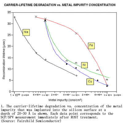
A single ROST measurement of lifetime provides a reliable assessment of metal impurity to readily distinguish between levels of 1011 cm-2 and 1012 cm-2.
A single lifetime value gives information of the level of the total subsurface contamination, but it does not provide definitive information about a specific type of impurity. The follow-up "time delay" relaxation test is needed to elucidate the contamination type.1
Three possible locations of metal near the surface were considered: on the surface, in the subsurface SCR, and in the SiO2 film.
Metals on the silicon surface
Iron and sodium shallow-implanted wafers were examined by measuring recombination lifetime (Fig. 2a ) and Wd (Fig. 2b) as a function of time delay at room temperature before and after the single ROST/heating. Figure 2 shows typical relaxation curves for iron and sodium implanted wafers, as well as for a non-implanted wafer (curve c). The curves'' characteristic attributes help to realize a behavior of the contaminant and to distinguish between different impurities.
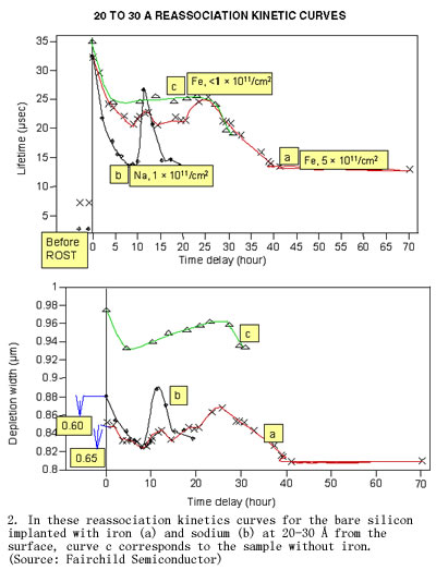
In the case of iron, the kinetics curves indicate the same time-dependent peculiarities that occur after heating (ROST); that is, the jump up of both lifetime and Wd right away after ROST, then the first decrease of both lifetime and depleted SCR, after that the small peak about 10 hours following heating, and afterwards the larger peak 20 to 25 hours after ROST.
The curve helps to understand that processes happening with iron atoms might be as follows: At room temperature, iron is predominantly positive and paired with boron (Fe+B-) in p-type silicon. The heating leads to the pair dissociation creating interstitial Fe+ and Feo atoms. They diffuse out of the SCR, resulting in the increase of lifetime and Wd
To diffuse iron, the pairs must first be dissociated. It has been found2 that the reassociation rate is less within the SCR than in the silicon bulk. Such a difference in pair formation rates within and beyond the SCR creates a concentration gradient of isolated atoms, which, in turn, provides the driving force for in-depth iron diffusion out of the SCR.
The further lifetime decrease at room temperature is explained by Fei+ returning back to the SCR. Interstitial Fe+ atoms diffuse towards B- atoms to electrostatically combine with them. It takes several hours to several days at room temperature, depending on the average distance between the ionized iron and the acceptor atoms. For NB=1015 cm-3, about 24 hours is the known time for Fe1,3,4 to reassociate with boron creating the stable shallow donor level Fe+B-. This explains the second peak on the reassociation curve (Fig. 2 ).
Generally, three charge states of FeB are possible: FeoB-, Fe+B- and Fe+Bo. The first peak in Figure 2 may be explained by the formation of the Fe+Bo pair with lower activation energy than Fe+B-.5 When associated, the lifetime increases because of the reduction of Fe+ recombination centers, and Wd increases because of a decrease in boron concentration that equals the increase in the concentration of FeB pairs. Thus, the lifetime peaks form the signature of iron contamination on the wafer surface.
In practice, it is not necessary to wait for several hours to identify the existence of an iron contaminant. A prior 80°C anneal for 20 minutes brings about the same effect of FeB association over a shorter period than required at room temperature.1,3
The lifetime relaxation curves are reversible; however, lifetime degrades less and less at room temperature after each repeated heating. This means that fewer Fe+ atoms return to the SCR, the rest being precipitated. This observation is useful to determine the effectiveness of the gettering technique. If gettering sites are present in the area where iron is diffused to, they will capture it and prevent it from returning to the original area.
The Fe-B pairs dissociate, and the Fe+ concentration increases at temperatures above 200°C. At sufficiently high temperatures, the Fermi level moves to the mid-gap position, and iron become mostly neutral. 6 However, at temperatures up to 700°C, the fraction of ionized iron remains high enough to make contaminant analysis possible. It gives the opportunity to measure the presence of iron in oxidation/diffusion furnaces. Metal can be detected on test wafers by the appearance of spots on the SPV wafer map with lower values of lifetime and depletion width. Contamination spots are of different size and number, depending on contamination severity.
Other contaminants, such as copper and sodium, are also distinguishable using the relaxation analysis described. When copper comes out on the wafer surface, the lifetime degrades very fast, reaching saturation in about two hours after heating at 210°C/3 min. In addition, the relaxation curve is not reversible, as in the case of iron. This separates copper contaminant from iron in SPV measurements. The phenomena are explained by the higher diffusivity of copper and the higher precipitation activity after in-diffusion. Sodium makes its signature by the appearance of a lifetime peak in ∼12 hours after ROST heating (Fig. 2 , curve b). This peak may be explained by the reactivity of sodium with the dopant, as iron does, or with another impurity, but the exact mechanism of such reactivity is still not known.
Metals in the silicon subsurface
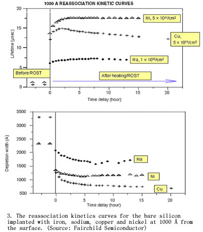
The same measurement technique was applied to bare silicon wafers implanted with copper, nickel and sodium at a depth of ∼1000 Å from the silicon surface (Fig. 3 ). The Wd extends to ∼3000 Å after implantation, before ROST annealing. Unlike the case when metallic ions are located on the surface, the lifetime is improved, and Wd becomes shallower after 210°C/3 min heating. The Wd is initially formed by both the surface and implanted charges. Metal diffuses in both directions during heating—to the surface and below to the silicon bulk out of the SCR where it precipitates. Lifetime increases and Wd shrinks because of the reduction in the number of Cu+, Ni+, or Na+ atoms that diffuse out of the SCR. The bulk-SCR lifetime dominates the surface lifetime at high impurity densities. The subsequent decrease of lifetime for copper may be explained by displacement of some atoms—recombination centers—towards the highly damaged layer, a better sink than the surface. Copper out-diffusion to the surface from the bulk is a known phenomenon.7
Metals in SiO2
Experiments were performed with oxidized wafers (oxide thickness of ∼1000 Å), which were intentionally implanted with metals to a depth of ∼100 Å from the oxide surface.b The lifetime and Wd, which are measured in silicon beneath the oxide, degrade depending on impurity concentration and oxide thickness (Fig. 4 ). The space charge, which equals the total oxide charge (QTOT), rises with increasing metal impurity concentration in the oxide.
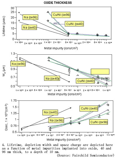
These experiments show that the presence of metal ions in the oxide causes the appearance of positive charges, likely metal ions, in the SCR
Low temperature annealing (applying ROST) is effective in increasing Wd and lifetime, and in decreasing QTOT (not shown in Fig. 4 ) . This is explained by the redistribution of metal ions in the oxide and the possible neutralization of metal charges caused by their reaction with oxide at elevated temperature. SCP parameter maps verify such redistribution.
A second set of experiments was implemented with test wafers processed at 950°C and higher in a furnace during wet oxidation, in the presence of a wafer intentionally contaminated with iron. Iron was detected by the appearance of localized spots with the degraded lifetime, as described. Iron has a strong interaction with the thermal SiO2 layer, which traps it. It is unclear which form of iron atoms serves as recombination centers, but it is obvious that iron is taken into the thermal SiO2 layer during oxide growth.
A special test was carried out with an iron-contaminated oxidized wafer. The SPV signal was insignificant caused by too small Wd because of strong contamination. The SPV measurement, followed by heating (ROST), manifested a significant value of Wd as well as an occurrence of distinctive spots of contaminant on the SCP map. This means that even low temperature annealing at 210°C/3 min initiates positive charges that enhance an appropriate Wd. Removing the oxide resulted in substantial improvement of lifetime and the disappearance of any contaminant spots on the map. Thus, iron exhibits a strong tendency to segregate into SiO2 or, at least, in the Si-SiO2 interface that is confirmed by other authors.8-10 About 75% of iron remains in the oxide layer even after annealing at 1150°C.8
Iron transport through SiO2 is largely dependent on the diffusion ambient, temperature and oxide thickness.6 An nitrogen ambient causes the diffusion of 70 to 100% of the surface contamination into the bulk. Hydrogen (wet oxidation) reduces iron''s reaction with oxygen or SiO2, allowing iron to remain mobile and diffuse into the substrate. Redistribution and precipitation behavior of copper and nickel during oxidation was shown to be dependent on the substrate type.10 Copper atoms tend to diffuse almost totally into the p-type silicon bulk8 while expected to pile up at the n-type Si/SiO2 interface during annealing. 7,10 Spectroscopic analysis showed sodium concentrating near the Si-SiO2 interface. It is interesting to note that the extra amount of Na+ implanted into SiO2/Si and then processed through oxidation was revealed neither by the SCP nor by conventional CV/TVS measurements. This means that Na+ mobile ions diffuse out of SCR area during oxidation.
Monitoring results
Metal surface contaminant can be successfully monitored through different steps of silicon processing using the SCP/SPV technique. The qualification parameters are recombination lifetime and Wd. Of special interest is the inspection of the silicon subsurface under SiO2. As long as oxide is transparent to the applied light, the stable interface charges will initiate an SPV signal, and most metals have a tendency to conglomerate near the Si-SiO2 interface. SiO2 traps and keeps iron in the oxide.
Single lifetime value gives some information of total subsurface contamination level, but it does not provide definitive information about a specific impurity. This may be recognized by examination of impurity behavior during the relaxation period; that is, measuring the recombination lifetime as a function of time at room temperature followed by preheating. The "relaxation" technique allows determination of the contamination type and reveals the behavior/redistribution of a contaminant in close proximity to the active device region. This depends on where the contaminant is located, whether on the surface, in the subsurface space charge region, or in the SiO2.
The results allow inline monitoring of metal impurity in diffusion/oxidation furnaces. The slope of the relaxation curve and the time of the lifetime degradation are dissimilar for iron, sodium and copper. Copper moves faster, and will likely precipitate on the surface. Thus, lifetime degradation for copper lasts as little as two hours, with an irreversible relaxation curve. The degradation of lifetime for iron and sodium lasts longer and is reversible. Another distinguishable feature is that iron and sodium have a characteristic time when lifetime increases (peaks on the reassociation curves), which are different for iron and sodium.
Acknowledgement
The author is grateful to Herb Robertson for his encouragement on this work, helpful discussions, and continuous support. The author also thanks Kathy Jenkins and Amit Pradhan for their active contribution to experiments. A special thanks goes to Edward Tsidilkovski, of QC Solutions Inc. for many useful discussions.
Footnotes
a. A special rapid optical surface treatment (ROST) heats the wafer to 210°C by illumination, maintains the temperature for three minutes, and then rapidly cools down to room temperature.
b. There is no necessity in ROST when lifetime is measured on oxidized wafers, because the SPV signal is initiated by the interface positive charges. It was tested that with no impurities, the magnitude of Wd and lifetime are the same for both ROST and no-ROST measurement.
References
1.Y. Sokolov, "Using Re-Association Kinetics to Identify Impurities in p-Type Silicon," Solid State Technology, September 2004.
2.K.L. Beaman et al., "Lateral Diffusion and Capture of Iron in p-Type Silicon," Materials Research Society Symp. Proc., 1995, Vol. 378, p. 291.
3.J. Lagowski et al., "Iron Detection in the Part Per Quadrillion Range in Silicon Using SPV and Photodissociation of Iron-Boron Pairs," Appl. Physics Letters, 1993, Vol. 63, No. 29, p. 3043.
4.W.B. Henley et al., "Detection of Copper Contamination in Silicon by Surface Photovoltage Length Measurement," Appl. Physics Letters, 1999, Vol . 74, No. 2, p.278.
5.K. Graff et al., "The Properties of Iron in Silicon," J. of the Electrochemical Society: Solid-State Science and Technology, 1981, Vol. 128, No. 3, p. 669.
6.A.A. Istratov et al., "Iron and its Complexes in Silicon," Appl. Physics A-Materials Science & Processes, 1999, Vol. 69, p. 13.
7.A. Istratov et al., "Physics of Copper in Silicon," J. of the Electrochemical Society, 2002, Vol. 149, No.1, p. G21.
8.M. Hourai et al., "Behavior of Defects Induced by Metallic Impurities on Si(100) Surfaces," Japanese J. of Appl. Physics, 1989, Vol. 28, No.12, p. 2413.
9.S. Sadamitsu et al., "Transmission Electron Microscopy Observation of Defects Induced by Fe Contamination on Si(100) Surface," Japanese J. of Appl. Physics, 1991, Vol. 30, No. 8, p.1591.
10.A.L. Rotondaro et al., "Impact of Fe and Cu Contamination on the Minority Carrier Lifetime of Silicon Substrates," J. of the Electrochemical Society, 1996, Vol. 143, No.9, p. 3014.