PIC24F 系列:16-Bit Flash Microcontrollers with USB On-The-Go (OTG)
This document contains device-specific information for the following devices:
. PIC24FJ64GB106 . PIC24FJ192GB108
. PIC24FJ128GB106 . PIC24FJ256GB108
. PIC24FJ192GB106 . PIC24FJ64GB110
. PIC24FJ256GB106 . PIC24FJ128GB110
. PIC24FJ64GB108 . PIC24FJ192GB110
. PIC24FJ128GB108 . PIC24FJ256GB110
Power Management:
. On-Chip 2.5V Voltage Regulator
. Switch between Clock Sources in Real Time
. Idle, Sleep and Doze modes with Fast Wake-up and Two-Speed Start-up
. Run mode: 1 mA/MIPS, 2.0V Typical
. Sleep mode Current Down to 100 nA Typical
. Standby Current with 32 kHz Oscillator: 2.5uA, 2.0V typical
Universal Serial Bus Features:
. USB v2.0 On-The-Go (OTG) Compliant
. Dual Role Capable . can act as either Host or Peripheral
. Low-Speed (1.5 Mb/s) and Full-Speed (12 Mb/s) USB Operation in Host mode
. Full-Speed USB Operation in Device mode
. High-Precision PLL for USB
. Internal Voltage Boost Assist for USB Bus Voltage Generation
. Interface for Off-Chip Charge Pump for USB Bus Voltage Generation
. Supports up to 32 Endpoints (16 bidirectional):
- USB Module can use any RAM location on the device as USB endpoint buffers
. On-Chip USB Transceiver with On-Chip Voltage Regulator
. Interface for Off-Chip USB Transceiver
. Supports Control, Interrupt, Isochronous and Bulk Transfers
. On-Chip Pull-up and Pull-Down Resistors
High-Performance CPU:
. Modified Harvard Architecture
. Up to 16 MIPS Operation at 32 MHz
. 8 MHz Internal Oscillator
. 17-Bit x 17-Bit Single-Cycle Hardware Multiplier
. 32-Bit by 16-Bit Hardware Divider
. 16 x 16-Bit Working Register Array
. C Compiler Optimized Instruction Set Architecture with Flexible Addressing modes
. Linear Program Memory Addressing, Up to 12 Mbytes
. Linear Data Memory Addressing, Up to 64 Kbytes
. Two Address Generation Units for Separate Read and Write Addressing of Data Memory
Analog Features:
. 10-Bit, Up to 16-Channel Analog-to-Digital (A/D) Converter at 500 ksps:
- Conversions available in Sleep mode
. Three Analog Comparators with Programmable Input/Output Configuration
. Charge Time Measurement Unit (CTMU)
Peripheral Features:
. Peripheral Pin Select:
- Allows independent I/O mapping of many peripherals at run time
- Continuous hardware integrity checking and safety interlocks prevent unintentional configuration changes
- Up to 44 available pins (100-pin devices)
. Three 3-Wire/4-Wire SPI modules (supports 4 Frame modes) with 8-Level FIFO Buffer
. Three I2C. modules support Multi-Master/Slave modes and 7-Bit/10-Bit Addressing
. Four UART modules:
- Supports RS-485, RS-232, LIN/J6202 protocols and IrDA®
- On-chip hardware encoder/decoder for IrDA
- Auto-wake-up and Auto-Baud Detect (ABD)
- 4-level deep FIFO buffer
. Five 16-Bit Timers/Counters with Programmable Prescaler
. Nine 16-Bit Capture Inputs, each with a Dedicated Time Base
. Nine 16-Bit Compare/PWM Outputs, each with a Dedicated Time Base
. 8-Bit Parallel Master Port (PMP/PSP):
- Up to 16 address pins
- Programmable polarity on control lines
. Hardware Real-Time Clock/Calendar (RTCC):
- Provides clock, calendar and alarm functions
. Programmable Cyclic Redundancy Check (CRC) Generator
. Up to 5 External Interrupt Sources
Special Microcontroller Features:
. Operating Voltage Range of 2.0V to 3.6V
. Self-Reprogrammable under Software Control
. 5.5V Tolerant Input (digital pins only)
. Configurable Open-Drain Outputs on Digital I/O
. High-Current Sink/Source (18 mA/18 mA) on all I/O
. Selectable Power Management modes:
- Sleep, Idle and Doze modes with fast wake-up
. Fail-Safe Clock Monitor Operation:
- Detects clock failure and switches to on-chip, low-power RC oscillator
. On-Chip LDO Regulator
. Power-on Reset (POR), Power-up Timer (PWRT), Low-Voltage Detect (LVD) and Oscillator Start-up Timer (OST)
. Flexible Watchdog Timer (WDT) with On-Chip.
Low-Power RC Oscillator for Reliable Operation
. In-Circuit Serial Programming. (ICSP.) and In-Circuit Debug (ICD) via 2 Pins
. JTAG Boundary Scan and Programming Support
. Brown-out Reset (BOR)
. Flash Program Memory:
- 10,000 erase/write cycle endurance (minimum)
- 20-year data retention minimum
- Selectable write protection boundary
- Write protection option for Flash Configuration Words
mTouch™ Capacitive Evaluation Kit
The mTouch Capacitive Evaluation Kit provides a simple platform for developing a variety of capacitive touch sense applications. Two motherboards are included in the kit, which connect to the 4 sensor boards.
This Capacitive Evaluation Kit is intended to be used to develop sensors and software using Microchip’s mTouch technologies. It is used by first connecting a sensor board, and then supplying power to the board via USB, Pickit™ 2, or Pickit Serial Analyzer.
The connector on the right side, with numbers 0 to 15, is the connector for sensing channels. The number, from 0 to 15, represents the microcontroller’s sensing channel.
The vertical 2-row header is for debugging, to give easy access to some of the microcontroller pins. Debugging may also be done by Microchip Programmers, or by I2C™ or USB with the mTouch Diagnostic Tool.
When using the evaluation kit out of the box, the LEDs default function is to illuminate on a key press. All functionalities may be reprogrammed by using a Microchip programmer, and reprogramming the firmware in the device. The firmware supplied with the evaluation kit has been written to use the four sensor boards supplied.
The USB connection supplies power to the board; no additional external power supply is needed. For independent operation, the evaluation board may be disconnected from the PC and powered at test points for independent functionality. For the PIC24F board,the USB also provides communications. The PIC16F board uses the PICkit Serial Analyzer to communicate via I2C to the PC. The PC side application that accompanies the evaluation kit allows users to monitor the performance of the touch sensors and calibrate their response. A separate, 6-wire programming interface allows users to replace the preprogrammed demo firmware with their own applications using Microchip’s MPLAB Integrated Development Environment and In-Circuit Serial Programming™ (ICSP™). This allows the board to also be used as a test bed for capacitive touch sense solutions.
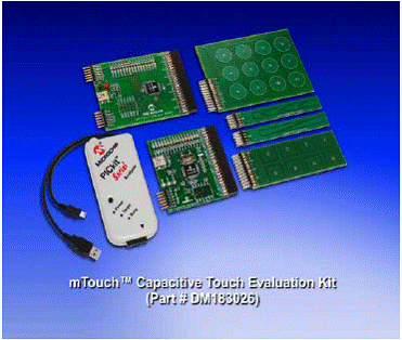
图1. mTouch评估板外形图
KIT CONTENTS:
• PIC16F727 CSM Motherboard
• PIC24FJ64GB106 Motherboard
• Direct 8 Key Board
• 12-Key Matrix Sensor Board
• 4-Channel Slider Sensor Board
• 2-Channel Slider Sensor Board
• PICKit Serial Analyzer
• USB Cable
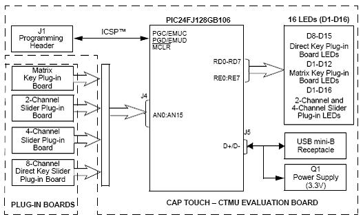
图2.CTMU板应用侧方框图
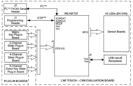
图3.CSM板应用侧方框图
图4.CAP TOUCH – CTMU 评估板方框图
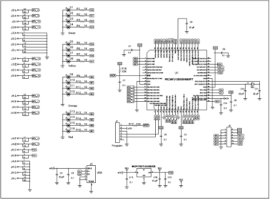
图5.mTouch™ – CTMU 评估板电路图
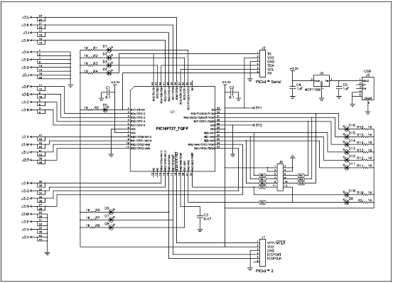
图6.mTouch™ – CSM 评估板电路图