Xilinx 公司的Spartan-6 FPGA是新一代低成本Spartan 现场可编程门阵列(FPGA)系列产品, 在成本、性能和开发硬件/工具方面实现了完美的平衡,可为消费、汽车、监控、无线以及其它成本敏感型市场设计更多创新的终端产品,如汽车信息娱乐, 平板显示器和视频监控等,通过降低多达50%的功耗来降低系统成本。本文介绍了Spartan-6 FPGA系列的主要特性, SP601开发板特性框图, SP601开发板框图和详细电路图.
The Spartan-6 FPGA family delivers an optimal balance of low risk, low cost, low power, and high performance for cost-sensitive applications. Built on a proven, low-power 45nm, 9-metal copper layer, dual-oxide process technology, the sixth generation in the Spartan-series offers advanced power management technology, up to 150,000 logic cells, integrated PCI Express® blocks, advanced memory support, 250 MHz DSP slices and 3.125 Gbps low-power transceivers.
The Spartan®-6 family provides leading system integration capabilities with the lowest total cost for high-volume applications. The thirteen-member family delivers expanded densities ranging from 3,400 to 148,000 logic cells, with half the power consumption of previous Spartan families and faster, more comprehensive connectivity. Built on a mature 45 nm low-power copper process technology that delivers the optimal balance of cost, power, and performance, the Spartan-6 family offers a new, more efficient, dual-register 6-input look-up table (LUT) logic and a rich selection of built-in system-level blocks. These include 18 Kb (2 x 9 Kb) block RAMs, second generation DSP48A1 slices, SDRAM memory controllers, enhanced mixed-mode clock management blocks, SelectIO™ technology, power-optimized highspeed serial transceiver blocks, PCI Express™ compatible Endpoint blocks, advanced system-level power management modes, autodetect configuration options, and enhanced IP security with AES and Device DNA protection. These features provide a low-cost programmable alternative to custom ASIC products with unprecedented ease-of-use. Spartan-6 FPGAs offer the best solution for highvolume logic designs, consumer-oriented DSP designs, and cost-sensitive embedded applications. Spartan-6 FPGAs are the programmable silicon foundation for Targeted Design Platforms that deliver integrated software and hardware components to enable
designers to focus on innovation as soon as their development cycle begins.
Spartan-6 FPGA 主要特性:
• Spartan-6 Family:
− Spartan-6 LX FPGA: Logic optimized
− Spartan-6 LXT FPGA: High-speed serial connectivity
• Designed for low cost
− Multiple efficient integrated blocks
− Optimized selection of I/O standards
− Staggered pads
− High volume plastic wire-bonded packages
• Low static and dynamic power
− 45 nm process optimized for cost and low power
− Hibernate power-down mode for zero power
− Suspend mode maintains state and configuration with multi-pin wake-up, control enhancement
− Lower-power 1.0V core voltage (LX FPGAs, -1L only)
− High performance 1.2V core voltage (LX and LXT FPGAs, -2 and -3 speed grades)
• Multi-voltage, multi-standard SelectIO banks
− Up to 1050 Mb/s data transfer rate per differential I/O
− Selectable output drive, up to 24 mA per pin
− 3.3V to 1.2V I/O standards and protocols
− Low-cost HSTL and SSTL memory interfaces
− Hot swap compliance
− Adjustable I/O slew rates to improve signal integrity
• High-speed GTP serial transceivers in the LXT FPGAs
− Up to 3.125 Gb/s
− High speed interfaces including: Serial ATA, Aurora, 1G Ethernet, PCI Express, OBSAI, CPRI, EPON, GPON, DisplayPort, and XAUI
• Integrated Endpoint block for PCI Express designs (LXT)
• Low cost PCI® technology support compatible with the 32 bit, 33 MHz specification
• Efficient DSP48A1 slices
− High-performance arithmetic and signal processing
− Fast 18 x 18 multiplier and 48-bit accumulator
− Pipelining and cascading capability
− Pre-adder to assist filter applications
• Integrated Memory Controller blocks
− DDR, DDR2, DDR3, and LPDDR support
− Data rates up to 800 Mb/s (12.8 Gb/s peak bandwidth)
− Multi-port bus structure with independent FIFO to reduce design timing issues
• Abundant logic resources with increased logic capacity
− Optional shift register or distributed RAM support
− Efficient 6-input LUTs improve performance and minimize power
− LUT with dual flip-flops for pipeline centric applications
• Block RAM with a wide range of granularity
− Efficient block RAM
− Fast block RAM with byte write enable
− 18 Kb blocks that can be optionally programmed as two independent 9 Kb block RAMs
• Clock Management Tile (CMT) for enhanced performance
− Low noise, flexible clocking
− Digital Clock Managers (DCMs) eliminate clock skew and duty cycle distortion
− Phase-Locked Loops (PLLs) for low-jitter clocking
− Frequency synthesis with simultaneous multiplication, division, and phase shifting
− Sixteen low-skew global clock networks
• Simplified configuration, supports low-cost standards
− 2-pin auto-detect configuration
− Broad third-party SPI (up to x4) and NOR Flash support
− Feature rich Xilinx Platform Flash with JTAG
− MultiBoot support for remote upgrade with multiple bitstreams, using watchdog protection
• Enhanced security for design protection
− Unique Device DNA identifier for design authentication
− AES bitstream encryption in the larger devices
• Faster embedded processing with enhanced, low cost, MicroBlaze™ soft processor
• Industry-leading IP and reference designs
Spartan-6 FPGA 系列产品型号:
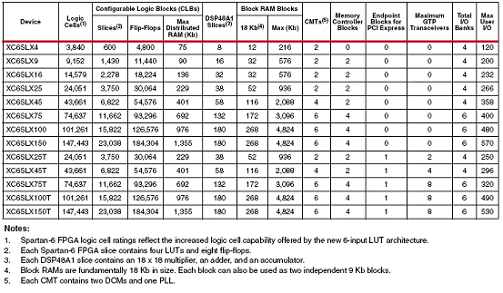
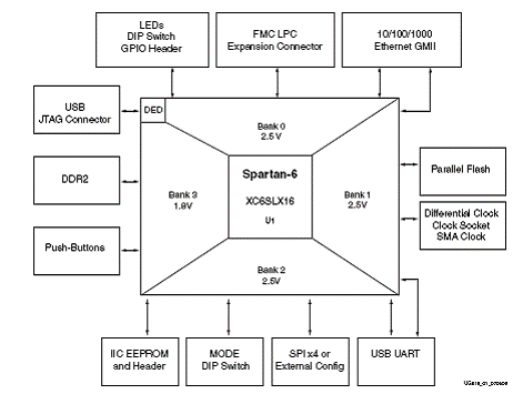
图1.SP601开发板特性框图
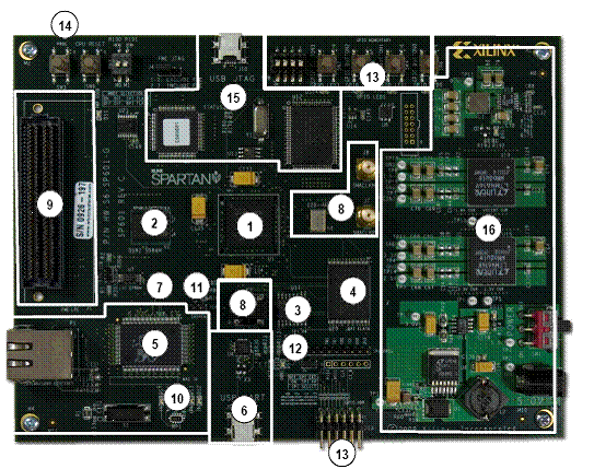
图2.SP601开发板外形图
SP601主要特性:
The SP601 board provides the following features:
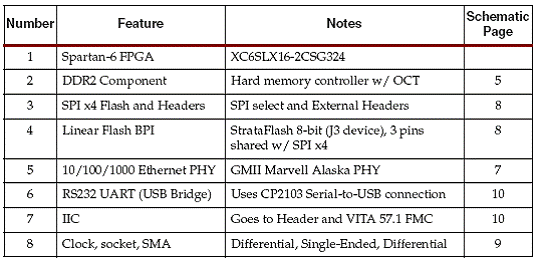
• 1. Spartan-6 XC6SLX16-2CSG324 FPGA
• 2. 128 MB DDR2 Component Memory
• 3. SPI x4 Flash
• 4. Linear Flash BPI
• 5. 10/100/1000 Tri-Speed Ethernet PHY
• 7. IIC Bus
♦ 8Kb NV Memory
♦ External Access 2-pin header
♦ VITA 57.1 FMC-LPC connector
• 8. Clock Generation
♦ Oscillator (Differential)
♦ Oscillator Socket (Single-Ended, 2.5V or 3.3V)
• SMA Connectors (Differential)
• 9. VITA 57.1 FMC-LPC Connector
• 10. Status LEDs
♦ FPGA_AWAKE
♦ INIT
♦ DONE
• 13. User IO
♦ User LEDs
♦ User DIP Switch
♦ User Push-Buttons
♦ GPIO Male Pin Header
• 14. FPGA_PROG_B Push-Button Switch
• Configuration Options
♦ 3. SPI x4 Flash (both onboard and off-board)
♦ 4. Linear Flash BPI
♦ JTAG Configuration
• Power Management - AC Adapter and 5V Input Power Jack/Switch, Onboard Power
Supplies
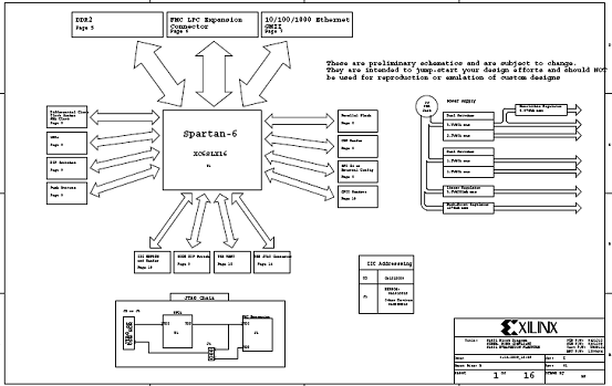
图3.SP601开发板框图
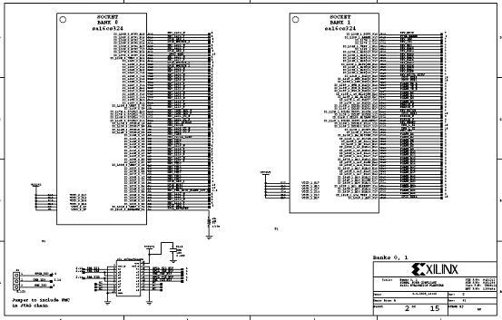
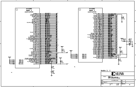
图4.SP601开发板电路图(1)
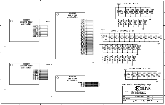
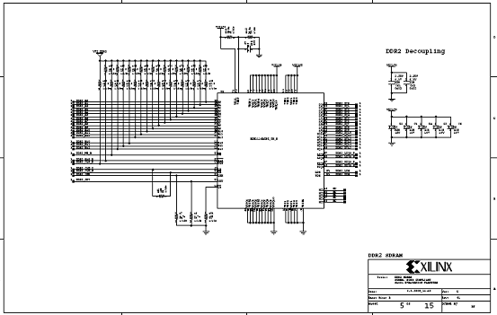
图5.SP601开发板电路图(2)
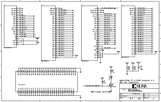
图6.SP601开发板电路图(3)
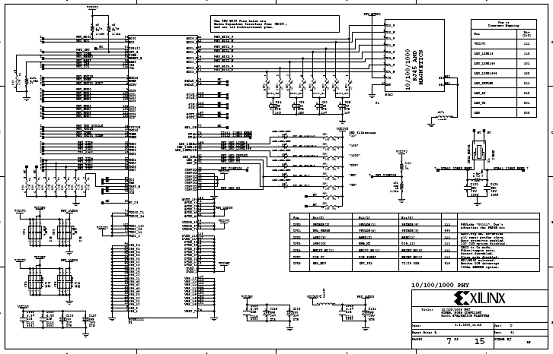
图7.SP601开发板电路图(4)
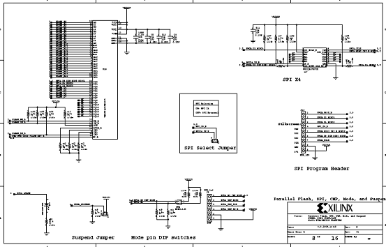
图8.SP601开发板电路图(5)
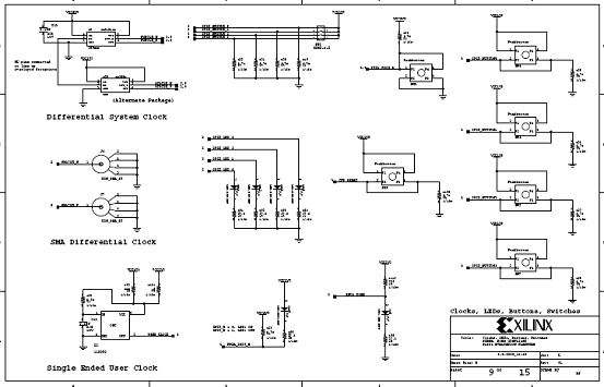
图9.SP601开发板电路图(4)
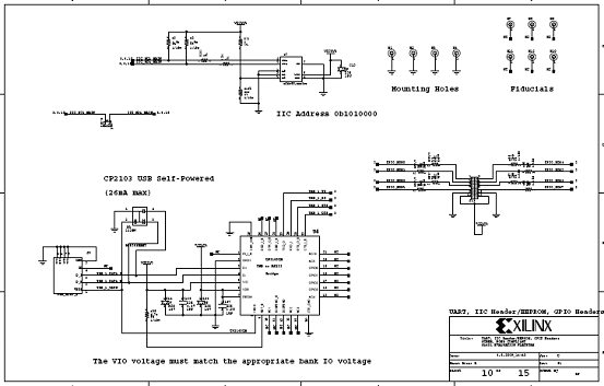
图10.SP601开发板电路图(5)
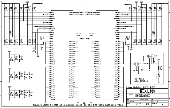
图11.SP601开发板电路图(6)
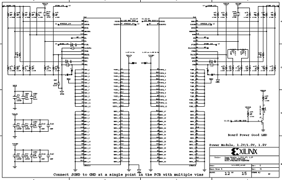
图12.SP601开发板电路图(7)
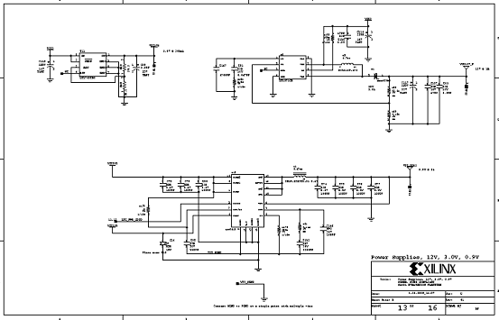
图13.SP601开发板电路图(8)
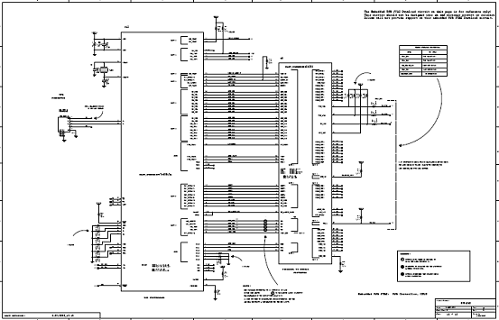
图14.SP601开发板电路图(9)
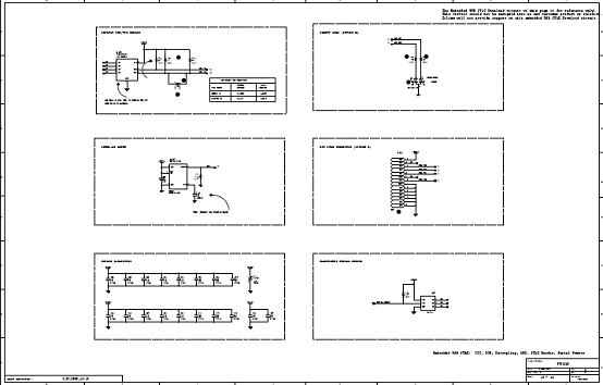
图15.SP601开发板电路图(10)
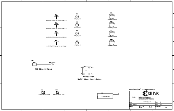
图16.SP601开发板电路图(11)
