Designers get the environment needed to achieve system-level power/performance estimation.
Today, one in five IC designs fail in tape-out due to power-related issues. For this reason, power management is considered a necessary part of every OEM and IC design flow. Also, there''s a growing interest in the evolution of power management techniques to address the challenges faced by system and IC designers. The goal of power management is to ensure all applications and operations in the OEM end product are properly (efficiently) powered and that the product is reliable.
| |
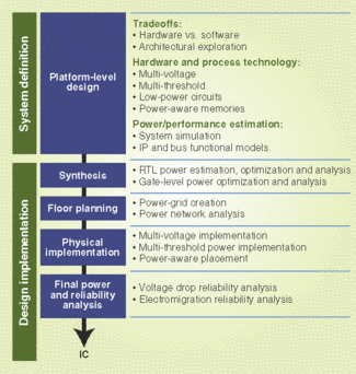 Figure power management in the design flow from an EDA perspective. |
The earliest power management decisions are made at the platform level during system definition (see the figure). At this point in the cycle, system designers make initial decisions about the end-product power requirements and distribution. That entails determining the overall power budget, making critical hardware/software tradeoffs, and working with designers to select the proper process technology for semiconductor fabrication, such as 90- verses 130-nm and multi-voltage/multi-threshold. EDA gives system designers the design and verification environment they need to achieve power/performance estimation at the system level. Such system-level decisions drive all subsequent software and semiconductor requirements.
Power at the IC level
Just as system-level decisions drive the semiconductor requirements, ICs together with process technology drive EDA tool and flow requirements. IC designers select EDA tools and flows for power management based on the following criteria:
- Process and application support (90 nm, multi-voltage, multi-threshold).
- Design optimization capabilities—needed to ensure operations stay within power budget.
- Design verification and signoff capabilities—needed to ensure device reliability and power integrity.
Leading EDA tools address all these requirements, offering power management throughout the design flow. The most effective EDA power management solutions are characterized by the ability to deliver comprehensive power estimation, optimization, analysis, and reliability signoff within a power-aware synthesis and signoff environment.
Power management
Unlike timing, which is localized to critical paths within the IC, power is distributed across the device. Power requirements are also dependent on the particular software application that''s running (application-specific) and the operating mode (mode-specific). In general, three areas of power need to be managed in the flow to ensure the design remains within the required power budget and reliability targets:
- Dynamic power. The designer must manage how much power is used when a circuit switches or is active (changes from 1 to 0 or 0 to 1) due to charging/discharging capacitance.
- Leakage (static) power. The designer must manage how much power "leaks" from transistors or is wasted when the circuit is static or unchanged.
- Peak power. The designer must manage peak-load periods.
To address these issues, power management techniques should be applied during every step of the flow, from design planning through reliability signoff analysis.
During synthesis, EDA helps designers complete RTL and gate-level power optimization together with peak and average power debug and analysis. Here, power management is needed to ensure the design''s dynamic and leakage power remain within the power budget and reliability targets. Power optimization and peak power analysis solutions include support for multi-voltage, multi-threshold, clock gating, data, and power-gating; RTL estimation analysis at full-chip/block level; and gate-level peak and average power analysis.
During floor planning, EDA helps designers create the power grid and perform power network analysis to assure the power remains within the power budget and reliability targets. Power-aware floor planning solutions today include support for power grid planning; multi-voltage region planning; clock tree planning; and estimation of voltage (IR) drop and electromigration effects.
During physical implementation (place and route), EDA helps designers implement power-saving features to manage both dynamic and leakage power in the design. Power implementation solutions today include support for multi-voltage and multi-threshold designs.
During reliability signoff analysis, EDA provides post-route analysis of power grids to detect power anomalies such as voltage drop and electromigration which, if left uncorrected, can lead to design failure.
Power management starts at the platform level and is driven by the OEM power budget requirements throughout the semiconductor value chain. IC designers collaborate closely with their EDA-tool providers to ensure power management is an integral part of their design flow.
EDA offers designers the much-needed infrastructure and tools for enabling power management throughout the flow. There are future opportunities for EDA to contribute to more power savings during system definition.
Rajiv Maheshwary is a senior director of marketing at Synopsys. He has more than 18 years of IC design and EDA experience and holds a BSEE degree from Worcester Polytechnic Institute and an MBA in marketing from San Jose State University. The company, based in Mountain View, CA, can be reached at (800) 541-7737, (650) 584-5000, or www.synopsys.com.
Wire-centric approaches ease IC development
To satisfy the market''s insatiable appetite for denser, faster, and smaller products, portable-device IC designers must become power-versus-feature-aware. While cramming lots of functions into one chip makes marketing happy, it leaves logic designers to contend with headaches like crosstalk, timing, congestion, and power consumption problems.
Today''s ultra-small geometries (130 nm and below) only exacerbate the problem. More cells in the design means more wire. And while many in the ASIC industry see design planning as the answer, it''s really only part of the equation. Getting to the crux of the problem will require early logic design planning along with new methodologies that place wire center stage during the planning, placement, routing, and optimization processes.
Unlike existing timing-driven approaches that don''t address wire length and are by themselves ineffective below 130 nm, wire-centric approaches excel with today''s deep-submicron process geometries. Timing-driven approaches require multiple iterations between logical and physical design teams. That isn''t feasible given today''s soaring ASIC costs, complexities, and shrinking geometries.
In contrast, wire-centric approaches tackle the underlying issues found in deep-submicron technologies. Wire is the predominant delay effect in these technologies. Therefore, it follows that reducing wire delay improves IC performance. The reduction of wire also allows smaller cells to be used, thereby reducing power consumption and die size. The reduction of wire lessens the potential of victim-aggressor situations that manifest as crosstalk failures as well as the total number of vias (which can simplify the manufacturing process).
Logic design engineers—who are intimate with the design and the means to floor plan, place, analyze, and subsequently optimize designs—should be part of the process prior to handoff to the physical implementation team. Logic designers can then use the methodologies to study block pin-outs, analyze cell compositions, determine fan-outs, measure logic levels, and make first-order "go" or "no go" decisions.
After reaching "go" decisions, logic designers can use floor planning techniques to examine the feasibility of various RAM placements (adjusting aspect ratios as needed), obtain feedback on block-size selection, and analyze block-level pin-outs in relation to block floor plans. During placement, wire-centric methodologies are used to place standard cells based on derived floor plans. Analysis would provide post-placement feedback on design implementation and let logic designers easily identify badly architectured or synthesized structures or global and localized congestion issues.
Finally, optimization routines would attack wire lengths and drive strengths first, followed by timing. The key is optimizing physical defects before beginning timing optimization because the physical defects could make timing optimization all but impossible.