摘要:在狭窄的金属线上,由尺寸效应引起的不断增加的电阻率难以避免。我们需要修改设计规则来加以改善。
Even materials that seem well known and familiar by day-to-day acquaintance sometimes give a reason for surprise. For example, copper is known as one of the best electrical conductors among metals, with a resistivity of 1.75 µΩ·cm at room temperature, beaten only by silver with a resistivity of 1.7 µΩ·cm. But the electrical properties of copper change when the material is integrated into very fine structures
. If the lateral dimensions of the copper are scaled to values that are ~100 nm or less, the resistivity increases significantly. For a 50 nm narrow wire, the resistivity is roughly a factor of 2 higher than the bulk value.
The semiconductor technologist must not neglect this observation because it has important consequences on certain figures of merit of VLSI circuits. First of all, the voltage drop in narrow interconnects will increase significantly. Second, the delay for signal propagation that is determined besides other parameters by the parasitic capacity and resistance of the local interconnects will be increased and will limit circuit performance. Third, the self-heating of the interconnect will be aggravated because the contribution caused by Joule heating will be larger. Size effects will definitely lower the margin for the maximum allowable current density during use that is determined by the reliability requirements of the metallization system. In summary, the technology parameters that enter the design process of a VLSI chip need to be reviewed.
In the past few years, numerous investigations were triggered in this field. Also, in the 2004 edition of the International Technology Roadmap for Semiconductors (ITRS),1 the electrical size effect found its way into the requirements for local, intermediate and global interconnects. To minimize the technological risks, it has been proven indispensable to characterize the size effect and also to understand its physical origin. In the following article, we concentrate on copper interconnects manufactured with a damascene technology. We present electrical results of lines that are 40-1000 nm wide and 50-230 nm high. Furthermore, we introduce a physically based model and use it to analyze the obtained experimental data.
Take a brief look at the roots of the electrical resistance in a conductor: The resistance is caused by the scattering of the charge carriers on imperfections of the metal. These may be static defects, like chemical impurities, or dynamic defects, like thermal vibrations of the lattice. The mean free path of the charge carriers is the traveling distance between two scattering events. For copper, this length is ~40 nm at room temperature. In very fine structures, the charge carriers are scattered additionally at the sidewalls of the structure (Fig. 1 ). Actually, this kind of scattering is always present, and it affects charge carriers, which are within a distance to the sidewall of a mean free path or less. In large, macroscopic wires of the fraction of electrons affected is negligible, so no size effect can be observed there.
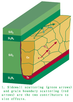
But scattering at sidewalls is not the whole story. It is observed that the seemingly homogeneous structure of copper is composed of tiny, individual grains. Typically, the extension of a copper grain is comparable to the width of the interconnect structure. The interfaces between neighboring grains also represent scattering sites for the charge carriers on their way through the conductor. Grain boundary scattering is the second contributor to size effects (Fig. 1 ). Again, the effect is significant for lateral grain dimensions comparable to the mean free path of the charge carriers and below. In brief, the electrical resistivity of an interconnect structure increases with both decreasing linewidth and decreasing grain size.
How is this qualitative picture of electron scattering translated into a mathematical framework? For sidewall scattering, the model of Fuchs-Sondheimer is frequently used,2 especially in its approximate form:
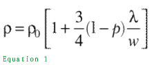
Hereby ρ0 is the resistivity of the bulk material, ρ the specular reflectivity, w the width of the interconnect structure and λ the mean free path of the conductor material. p is the fraction of the elastically scattered electrons at the sidewalls. It assumes values between 0 and 1. "p = 1" means all electrons are scattered in an elastic way, and no resistivity increase caused by sidewall scattering occurs.
Strictly speaking, Equation 1 is valid for structures with square or circular cross-sectional areas where the linewidths are significantly larger than the mean free path. For smaller widths or other line geometries, a more complicated equation applies.
To complete the picture we need to consider the contribution that describes grain boundary scattering.3 According to Matthiessen''s rule, the contributions from sidewall scattering and grain boundary scattering can simply be added and the measured resistivity can be described by a combined compact model.:4,5
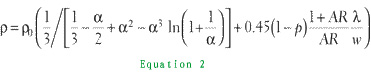
when

The first term of the sum in the bracket describes the scattering at the grain boundaries; d is the average distance between grain boundaries, and R is the reflection coefficient of the grain boundaries. R may assume values between 0 and 1 with "R = 0" meaning no grain boundary scattering.
The second term is a more precise description of the scattering at the sidewall than described by Equation 1 . Instead of a dependence only of the linewidth w, the aspect ratio (AR) is also implemented as a parameter and allows a more detailed description of line geometry.
The first term in Equation 2 is determined by grain size d, the second term by linewidth w. Grain size in turn is comparable to linewidth in damascene metallization schemes with tight feature sizes.6,7 Therefore, both contributions are finally determined by the CD of the technology.
Since the two contributions in Equation 2 have a different functional dependence on the linewidth w, they can be separated.
What do electrical data of nanometer-scale interconnects look like? Figure 2 shows the dependence of the electrical resistivity of copper interconnects on linewidth. The structures were manufactured by an adaptation8 of a standard damascene process. In Figure 2, the fit curve obtained with the compact model of Equation 2 is also shown, demonstrating an excellent agreement between model and experiment. Furthermore, the individual contributions to electrical resistivity resulting from sidewall scattering and grain boundary scattering are displayed.
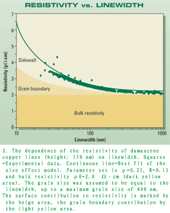
Using this analysis, the question may be answered by what the dominating effect causing the size effect in copper damascene interconnects is. For the narrow lines, sidewall scattering, as well as grain boundary scattering, contribute roughly equally to the increase of the resistivity. The picture seems to change for wider lines, where only sidewall scattering can be observed. However, the lines investigated in this case had a thickness of only 150 nm, so even for the wide lines a significant contribution of sidewall scattering from top and bottom surfaces is present.
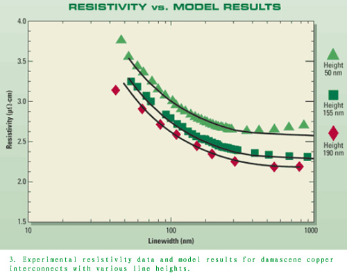
The versatility of the compact model to handle different line geometries is demonstrated in Figure 3 , where the resistivity data of different sample sets with line thicknesses ranging from 50 to 190 nm are shown. The fits shown were obtained with nearly identical values for ρ, R, and ρ0, and are in excellent agreement with the data.
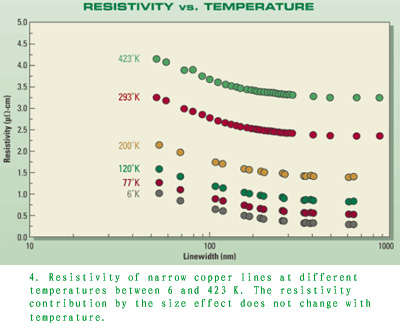
Would it be possible to reduce the resistivity by cooling the samples? After all, the bulk resistivity of most metals can be reduced to almost zero by cooling to sufficiently low temperatures. As discussed above, the resistivity in metals consists of two parts: the scattering of charge carriers at lattice vibrations — this is the temperature-dependent part — and the scattering of charge carriers at defects like impurities and, in the case of narrow wires, also at sidewalls and grain boundaries. The latter parts are independent of temperature, at least in a first-order approximation.
So in all wires made of the same material, no matter what size, a temperature change will alter the resistivity always by the same amount, which is given by the change of electron scattering at lattice vibrations. In clean bulk samples, where this is the main contribution, the resistivity can be reduced to almost zero by cooling. In narrow interconnects, however, the temperature-independent contribution dominates and therefore the relative reduction of resistivity, which can be obtained by cooling, is smaller. This is confirmed by experimental results, in which wires of various sizes were cooled down to 4 K (Fig. 4 ).
What do we learn from these observations? First, the resistivity increase is a basic physical phenomenon, and hence with today''s knowledge, there is no solution at hand. The root causes for this resistivity increase are additional scattering sites for the charge carriers that will come into play when scaling of the structures comes close to 100 nm or below for copper. There are aspects to scaling we have to live with, as there is no way to avoid the narrow linewidths in future technologies. What may be influenced are the interface properties that in the above consideration are hidden in the scattering parameter for the sidewall ρ and the grain boundary R; to be more precise, on the one hand, the sidewall between copper and dielectric material and, on the other hand, the boundary between two neighboring grains.
For future technology nodes we expect an aggravation of the size effect as projected by both our model and the experimental data obtained. This is quite obvious from applying the described model. Therefore, we think that it is indispensable to adapt the design rules to the scaling behavior of the resistance of interconnect levels and to take into account the size effect originated and increased resistivity values in the design manual for future chip generations.
Author InformationWerner Steinhoegl is staff expert in Infineon Technologies '' corporate research department. Since joining the company in 1998, he has held technical positions relating to the modeling of electrical and thermal properties of metallic conductors in the sub-100 nm range, as well as simulation of electrical properties of low-k dielectrics. Furthermore, he has been active in the simulation and modeling of semiconductor equipment and production processes including CVD, PECVD, PVD, electroplating and RTP. He also has expertise in analysis of nanoscale interconnects using focused ion beam. He has a diploma in physics from the Ludwig-Maximilian University in Munich, and a Ph.D. in physics from the Max-Planck-Institut für Strömungsforschung in Göttingen.
Guenther Schindler studied physics at the Technical University of Munich. After his Ph.D. thesis on Josephson junctions in grain boundaries of bulk HTSCs, he joined North Carolina State University in Raleigh, N.C., as a post-doctorate for further study of the Josephson properties HTSCs. He joined the Siemens semiconductor group in 1995 to work on the development of ferroelectric memories (FeRAM). During this project, he was assigned to Symetrix Corp. in Colorado Springs, Colo
., on a collaboration project. He joined Infineon Corporate Research in 2000 to work on his present field of nanointerconnects.
Manfred Engelhardt studied physics at the University of Regensburg, Germany, where he holds a Ph.D. in solid-state physics (1984). He then joined Siemens Semiconductors in Munich, Germany. His responsibilities in Central Research and in the Semiconductor Components Group included the development of plasma etching processes for the company''s memory and logic products. Since the foundation of Infineon Technologies in 1999, he has been with Corporate Research, where he heads the nanointerconnect project. He is an active member of the Electrochemical Society.
References1. The International Technology Roadmap for Semiconductors (ITRS), 2004 Update. Available at www.itrs.net/common/2004update/2004update.htm.
2. E.H. Sondheimer, "The Mean Free Path of Electrons in Metals," Adv. Phys., 1952.
3. A.F. Mayadas and M. Shatzkes, "Electrical-Resistivity Model for Polycrystalline Films: The Case of Arbitrary Reflection at External Surfaces," Phys. Rev. B, 1970, Vol. 1, p. 1382.
4. W. Steinhoegl, G. Schindler, G. Steinlesberger, M. Traving and M. Engelhardt, "Comprehensive Study of Copper Wires With Lateral Dimensions of 100 nm and Smaller," J. Appl. Phys., 2005, Vol. 97, p. 023706.
5. W. Steinhoegl, G. Schindler, G. Steinlesberger, M. Traving and M. Engelhardt, "Scaling Laws for the Resistivity Increase of sub-100 nm Interconnects," Proc. of the 2003 Int. Conf. on Simulation of Semiconductor Processes and Devices, 2003, p. 27.
6. G. Steinlesberger, et al., "Microstructure Study of Cu Damascene Nano-Interconnects," Proc. of the Advanced Metallization Conf. (AMC), 2002, p. 397.
7. G. Schindler, et al., "A Morphology Study of Copper and Aluminum Interconnects," Proc. of the Advanced Metallization Conf. (AMC), 2003, p. 213.
8. G. Steinlesberger, M. Engelhardt, G. Schindler and W. Steinhoegl, "Processing Technology for the Investigation of sub-50 nm Copper Damascene Interconnects," Solid State Electronics, 2002, Vol. 47, p. 1237
AcknowledgementThe authors thank G. Steinlesberger, M. Traving and W. Hoenlein for valuable contributions and discussions.
来源:半导体国际 作者: 时间:2005/8/15 0:00:00
